
Material Analysis and Testing: Essential for Manufacturing and Production
Our team consists of highly qualified and motivated professionals, who are all experts in their field. With many years of experience in the industry, they have the expertise to provide comprehensive, first-rate services to our clients.
✅ Expertise – Our team has professional skills and industry experience accumulated over many years.
⏱️ Quick Turnaround – We guarantee 100% on-time delivery of inspection reports.
💡 Comprehensive Support – We provide full support and solutions for any challenges you face.
🏆 Certified Quality – ISO/IEC 17025:2017
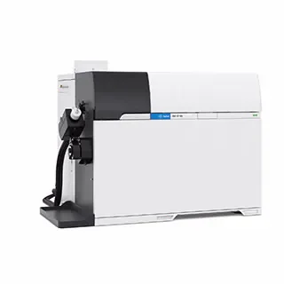
7900 ICP-MS
Inductively Coupled Plasma Mass Spectrometry (ICP-MS)
ICP-MS (Inductively Coupled Plasma Mass Spectrometry) is a high-sensitivity, high-resolution analytical technique used for detecting and quantifying elements in various samples.
Principle
A sample is introduced into the inductively coupled plasma, where it is exposed to high temperatures that ionize its atoms. These ions are then separated and detected based on their mass-to-charge ratio (m/z) in a mass spectrometer, allowing for precise elemental analysis.
Key Features
🔬 High Sensitivity – Capable of detecting ultra-trace element concentrations, with a dynamic range of up to 11 orders of magnitude, from ppt (parts per trillion) to percentage levels.
⚡ High Resolution – Utilizes a mass spectrometer to differentiate elements with similar masses, ensuring accurate identification.
🧪 Multi-Element Analysis – Can simultaneously detect multiple elements, making it ideal for environmental monitoring, biomedical research, and food safety testing.
⏩ Fast Analysis – The Agilent 7900 ICP-MS enables ultra-fast data acquisition, performing 10,000 independent measurements per second for real-time results.
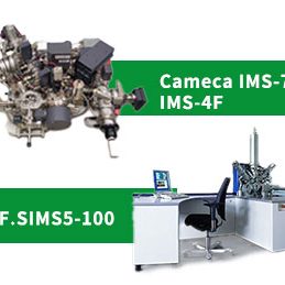
TOF.SIMS5-100
Secondary Ion Mass Spectrometry (SIMS)
Secondary Ion Mass Spectrometry (SIMS) is a highly sensitive surface analysis technique commonly used in semiconductors, materials science, life sciences, and geology. SIMS provides highly detailed information about the elemental composition and chemical structure of surfaces.
Features of SIMS
⚡ High Spatial Resolution
SIMS offers extremely high spatial resolution, reaching submicron or smaller scales, enabling precise analysis of tiny areas.
🔬 High Sensitivity
SIMS can detect elements at very low concentrations, typically in the range of parts per million (ppm) to parts per billion (ppb).
Surface Composition Analysis
SIMS is primarily used for surface analysis, providing detailed information on the composition and structure of material surfaces.
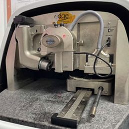
AFM
Atomic Force Microscope (AFM)
Atomic Force Microscope (AFM) is a high-resolution microscopy technique with a wide range of applications. It is a powerful tool for nanometer-scale research and applications across various fields, including materials science, biology, and nanotechnology.
Features
Patented Technology
The Dimension Edge AFM utilizes Bruker’s patented PeakForce Tapping® technology, delivering high-performance AFM capabilities among similar products.
Wide Applications
AFM can be adapted to different research directions with customized experimental setups and offers advanced nanometer-scale measurement capabilities.
Precision Measurement
AFM features low drift and low noise, enhancing data acquisition speed and reliability. Its integrated visual feedback and pre-configured settings ensure consistent, expert-level measurement results.
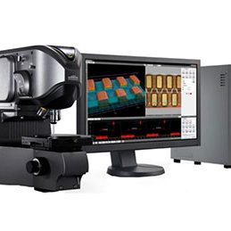
LSCM
Laser Scanning Confocal Microscope (LSCM)
Laser Scanning Confocal Microscope (LSCM) is an advanced optical imaging technology that provides high resolution, high contrast, and real-time observation capabilities. It is an indispensable tool in various fields, including materials science and biological research.
Principles and Features
Scanning System
LSCM includes a scanning system that uses lenses or prisms to direct the laser beam across the sample surface. By rapidly scanning a focused light source, LSCM can construct high-resolution images in three-dimensional space.
Confocal Technology
By utilizing confocal technology, the system ensures that only light from the focal plane reaches the detector, effectively eliminating scattered light from other parts of the sample. This results in enhanced image contrast and resolution.
3D Imaging
Due to its scanning capabilities, LSCM can capture images at different focal depths, allowing researchers to construct highly detailed 3D structures of samples.

XRD
High-Resolution X-ray Diffractometer (XRD)
A high-end instrument for materials analysis, the X-ray diffractometer (XRD) is widely used in advanced materials science, thin-film technology, semiconductor process development, and industrial research. It enables the study and measurement of crystal structures, crystalline phases, lattice parameters, and crystal size.
Key Features
⚡ High Resolution
- Provides exceptional resolution, allowing precise analysis of minute changes in crystal structures and characteristics.
Versatility
- Supports multiple analytical modes, including powder diffraction (XRD) and X-ray reflectometry (XRR), making it suitable for various sample types and applications.
Automation
- Equipped with an automated control system and high-throughput sample handling, enabling fast and efficient sample analysis.
Intelligent Data Analysis
- Features specialized data analysis software for comprehensive diffraction data processing, ensuring high-quality results.
Flexible Configuration and Expandability
- Can be customized and expanded according to user needs, accommodating different research and industrial applications.
Integrated X-ray Solution
- Ideal for industrial applications such as semiconductors, single-crystal wafers, polycrystalline solids, thin films, ultra-thin films, nanomaterials, and amorphous layers.
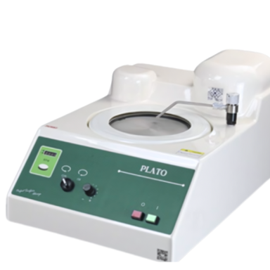
Plato
Damaged Layer Inspection and Analysis Service
Laser Scanning Confocal Microscope (LSCM) is an advanced optical imaging technology that provides high resolution, high contrast, and real-time observation capabilities. It is an indispensable tool in various fields, including materials science and biological research.
Principles and Features
Scanning System
LSCM includes a scanning system that uses lenses or prisms to direct the laser beam across the sample surface. By rapidly scanning a focused light source, LSCM can construct high-resolution images in three-dimensional space.
Confocal Technology
By utilizing confocal technology, the system ensures that only light from the focal plane reaches the detector, effectively eliminating scattered light from other parts of the sample. This results in enhanced image contrast and resolution.
3D Imaging
Due to its scanning capabilities, LSCM can capture images at different focal depths, allowing researchers to construct highly detailed 3D structures of samples.
Damaged Layer Inspection and Analysis Service
Damaged layers commonly occur during various stages of wafer processing, including:
- Ingot Diameter Grinding Machine → Damaged layer forms on the outer diameter of the ingot after grinding.
- Ingot Slicing Machine → Damaged layer appears on both surfaces of the sliced wafer.
- Wafer Grinding Machine → Damaged layer is present on both surfaces of the wafer after grinding.
By identifying and analyzing these damaged layers, precise adjustments can be made to optimize removal processes, ensuring high yield and minimal defects in semiconductor manufacturing.
Contact us
Telephone: +1 (858) 243-4766
E-mail: info@ameridx.com
Address: 9235 Activity Rd Suite 101, San Diego, CA 92126
2013-2025 © America Diagnostics. All rights reserved.
Together We Thrive !
America Diagnostics, 9235 Activity Road, Suite 101, San Diego, CA 92126 USA Tel: (858) 282-8567 Email: info@ameridx.com
We need your consent to load the translations
We use a third-party service to translate the website content that may collect data about your activity. Please review the details in the privacy policy and accept the service to view the translations.